Download
1 / 22
240 likes | 320 Vues
Explore basic fabrication steps, transistor structures, and behavior in VLSI technology. Learn about latch-up, fabrication processes, and transistor parasitics. Understand CMOS ICs, latch-up prevention, and solutions for proper circuit layout structures.

E N D
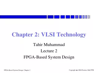
Chapter 2: VLSI Technology Tahir Muhammad Lecture 2 FPGA-Based System Design
Topics • Basic fabrication steps. • Transistor structures. • Basic transistor behavior. • Latch up.
Fabrication processes • IC built on silicon substrate: • some structures diffused into substrate; • other structures built on top of substrate. • Substrate regions are doped with n-type and p-type impurities. (n+ = heavily doped) • Wires made of polycrystalline silicon (poly), multiple layers of aluminum/copper (metal). • Silicon dioxide (SiO2) is insulator.
transistor via Simple cross section SiO2 metal3 metal2 metal1 poly substrate n+ n+ p+ substrate
Photolithography Mask patterns are put on wafer using photo-sensitive material:
Process steps First place tubs to provide properly-doped substrate for n-type, p-type transistors: p-tub n-tub substrate
Process steps, cont’d. Pattern polysilicon before diffusion regions: gate oxide poly poly p-tub n-tub
Process steps, cont’d Add diffusions, performing self-masking: poly poly p-tub n+ n+ n-tub p+ p+
Process steps, cont’d Start adding metal layers: metal 1 metal 1 vias poly poly p-tub n+ n+ n-tub p+ p+
Level 2 metal • Polish SiO2 before adding metal 2: metal 2 metal 1 metal 1 vias poly poly p-tub n+ n+ p-tub p+ p+
Transistor structure n-type transistor:
Transistor layout n-type (tubs may vary): L w
Drain current • Linear region (Vds < Vgs - Vt): • Id = k’ (W/L)(Vgs - Vt)(Vds - 0.5Vds2) • Saturation region (Vds >= Vgs - Vt): • Id = 0.5k’ (W/L)(Vgs - Vt) 2
90 nm transconductances Typical parameters: • n-type: • kn’ = 13 A/V2 • Vtn = 0.14 V • p-type: • kp’ = 7 A/V2 • Vtp = -0.21 V
Current through a transistor Use 90 nm parameters. Let W/L = 3/2. Measure at boundary between linear and saturation regions. • Vgs = 0.25V: Id = 0.5k’(W/L)(Vgs-Vt)2= 0.12 A • Vgs = 1V: Id = 7.2 mA
Basic transistor parasitics • Gate to substrate, also gate to source/drain. • Source/drain capacitance, resistance.
Basic transistor parasitics, cont’d • Gate capacitance Cg. Determined by active area. • Source/drain overlap capacitances Cgs, Cgd. Determined by source/gate and drain/gate overlaps. Independent of transistor L. • Cgs = Col W • Gate/bulk overlap capacitance.
Latch-up • CMOS ICs have parastic silicon-controlled rectifiers (SCRs). • When powered up, SCRs can turn on, creating low-resistance path from power to ground. Current can destroy chip. • Early CMOS problem. Can be solved with proper circuit/layout structures.
Parasitic SCR circuit I-V behavior
Solution to latch-up Use tub ties to connect tub to power rail. Use enough to create low-voltage connection.