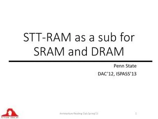
Evaluating STT-RAM as an Energy-Efficient Main Memory Alternative
230 likes | 385 Vues
Evaluating STT-RAM as an Energy-Efficient Main Memory Alternative. Emre K ü lt ü rsay * , Mahmut Kandemir * , Anand Sivasubramaniam * , and Onur Mutlu † * Pennsylvania State University † Carnegie Mellon University ISPASS-2013

Evaluating STT-RAM as an Energy-Efficient Main Memory Alternative
E N D
Presentation Transcript
Evaluating STT-RAM as an Energy-Efficient Main Memory Alternative Emre Kültürsay*, MahmutKandemir*, AnandSivasubramaniam*, and OnurMutlu† * Pennsylvania State University † Carnegie Mellon University ISPASS-2013 2013 IEEE International Symposium on Performance Analysis of Systems and Software April 23, 2013 Austin, TX
Introduction • Memory trends in data centers • More memory capacity, • Higher memory access rates. • Result • Increasing memory power, • Reports indicate 30% of overall power from memory. • Cost • Operational + acquisition costs = Total cost of ownership (TCO) • 30% power from memory: high operational cost of memory • How to reduce memory power? • DRAM? Alternative technology to DRAM? • (possibly) Higher acquisition cost, but • Reduced TCO by means of better energy efficiency. ISPASS 2013 - Kultursay et al.
Introduction • What technology to use? • Prior research focused: Flash or PCRAM as main memory. • (NAND) Flash • Enables running applications that require huge memory, • Very slow, incompatible block-based operation; not adopted widely. • PCRAM • Higher capacity than DRAM, • Performance and energy vs. DRAM: not very good • 2-4X read, 10-100X write performance; similar trend in energy. • STT-RAM • Considered as replacement for on-chip SRAM caches. • Main memory? Not evaluated. • vs. DRAM? Similar read latency and energy, slightly worse in writes. ISPASS 2013 - Kultursay et al.
Introduction • In this work, we ask: • Can we use STT-RAM to completely replace DRAM main memory? • For a positive answer, we need from STT-RAM: • Similar capacity and performance as DRAM • Better energy • Enough to offset potentially higher acquisition costs ISPASS 2013 - Kultursay et al.
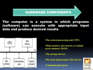
DRAM Basics CPU Memory Bus Memory Modules (DIMMs) • System: Cores, L2 caches, MCs over a network. • A MC controls one channel (one or more DIMMs). • A DIMM has many DRAM chips. • A DRAM request: Served by all chips simultaneously. Memory Controller L2 Cache Core + L1 Cache Channel … … Network … Memory Controller Core + L1 Cache L2 Cache Channel ISPASS 2013 - Kultursay et al.
DRAM Basics • A DRAM chip has multiple banks • Banks operate independently. • Banks share external buses. • Use row and column address to identify data in a bank. • High level DRAM operations: • Activate (ACT): Sense data stored in array, recover it in the row buffer. • Read (RD), Write(WR): Access row buffer (and bitlines, and cells, simultaneously). • Precharge(PRE): Reset bitlines to sensing voltage. • Refresh (REF): Read/Write each row periodically to recover leaking charges. Bit Line Memory Array Word Line Row Address Row Decoder Sense Amps (row buffer) Access Transistor Storage Capacitor Column Address Column Select Col. Decoder Read Latch Write Driver ISPASS 2013 - Kultursay et al.
STT-RAM Basics • Magnetic Tunnel Junction (MTJ) • Reference layer: Fixed • Free layer: Parallel or anti-parallel • Cell • Access transistor, bit/sense lines • Read and Write • Read: Apply a small voltage across bitline and senseline; read the current. • Write: Push large current through MTJ. Direction of current determines new orientation of the free layer. Word Line MTJ Access Transistor Logical 0 Sense Line Bit Line Reference Layer Barrier Free Layer Logical 1 Reference Layer Barrier Free Layer ISPASS 2013 - Kultursay et al.
Major DRAM/STT-RAM Differences • Dynamic memory • Charge in DRAM cell capacitor leaks slowly • Refresh or lose your data. • Need no refresh in STT-RAM (non-volatile) • Data stays (practically) forever (>10years). • Non-destructive (array) reads • DRAM (destructive) • PRE: Pull bitlines to Vbitline= Vcc/2; Data in cell: Vcell=0 or Vcell=Vcc • ACT: Charge shared across bitlines and cell capacitors. • Differential Sense: Vcc/2±V; then slowly recover to full value (0 or Vcc). • STT-RAM (non-destructive) • ACT: Does not disturb cell data. Copy array data to "decoupled row buffer". • RB can operate "independent" from the array when sensing is done. ISPASS 2013 - Kultursay et al.
Experimental Setup • Simulator • In-house instruction trace based cycle-level • Cores • Out-of-order model with instruction window • Maximum 3 instructions/cycle • Caches • 32KB L1 (2 cycles), 512KB L2 (12 cycles) • Memory • Channel, rank, bank, bus conflicts and bandwidth limitations • DDR3 memory timing parameters • 75/125 cycles RB hit and conflict, 25 cycles STT-RAM write pulse (10ns). • 1GB memory capacity; one channel ISPASS 2013 - Kultursay et al.
Energy Breakdown • Memory energy • Activity based model • Energy per memory activity • From modified CACTI models (DRAM and STT-RAM) • DRAM energy components • ACT+PRE: Switching from one row to another • RD+WR: Performing a RD or a WR operation that is a DRAM RB hit. • REF: Periodic refresh (background) • STT-RAM energy components • ACT+PRE: Switching the active row (similar to DRAM) • RB: Requests served from the RB (unlike DRAM, does not involve bitline charge/discharge: decoupled RB) • WB: Flushing RB contents to the STT-RAM array. ISPASS 2013 - Kultursay et al.
Workloads • Single-threaded applications • 14 applications from SPEC CPU2006 suite • Running on a uniprocessor • Multiprogrammedworkloads • 10 workload mixes • 4 applications on 4 cores • Simulation duration • 5 billion cycles • Equivalent to 2 seconds of real execution (at 2.5GHz) ISPASS 2013 - Kultursay et al.
Baseline DRAM Memory • Baseline DRAM main memory (1GB capacity). • IPC • 0.66 to 2.05 • Energy breakdown • ACT+PRE=62%, RD+WR=24%, REF=14%, on average. • Rest of the results will be normalized to • IPC and total energy with this DRAM main memory. ISPASS 2013 - Kultursay et al.
Baseline STT-RAM Memory • Unoptimized STT-RAM: Directly replace DRAM. • No special treatment of STT-RAM. • Performance: Degrades by 5%. • Energy: Degrades by 96% (almost 2X!). • REF (14%) eliminated. • WB dominates: high cost of STT-RAM writes. STT-RAM Main Memory: Not a good idea? ISPASS 2013 - Kultursay et al.
Optimizations for STT-RAM • How dirty is the row buffer? • Clean: 60% of the time. • Dirty>3: Only 6%. • Selective Write • One dirty bit per row buffer: skip writeback if clean. • Save energy by less writes; faster row switching possible. • Partial Write • More dirty bits: One dirty bit per cache block sized data • Write even less data upon RB conflict. ISPASS 2013 - Kultursay et al.
Optimizations for STT-RAM • A look at the row buffer hit rates: • Reads 81%, writes 64%. • Consider writes as : • Operations with less locality, • Operations that can be delayed more (less CPU stalls). • Write Bypass • Reads still served from row buffer. • Writes bypass the row buffer: do not cause RB conflicts, do not pollute RB. • RB is always clean: Just discard to get the next row. • No write-back: faster row switching. ISPASS 2013 - Kultursay et al.
Experimental Evaluation • Selective write • 1 dirty bit per row • Energy • 196% down to 108% • RB clean 60% of the time. • Partial Write • 1 dirty bit per 64B block • Energy • Down to 59% of DRAM. • Low dirtiness in RB. ISPASS 2013 - Kultursay et al.
Experimental Evaluation • Write Bypass: • Energy: 42% of DRAM. (with also partial write) • Performance of Optimized STT-RAM: • Partial write, write bypass • -1% to +4% variation. • +1% vs. DRAM, on avg. ISPASS 2013 - Kultursay et al.
Evaluation: Multiprogrammed Workloads • 4 applications executed together • On 4-cores; 1 MC with 4GB capacity • More memory pressure: shared bandwidth and row buffers. • Energy results without partial write and write bypass with partial write and write bypass • Down from 200% of DRAM to 40% of DRAM. ISPASS 2013 - Kultursay et al.
Evaluation: Multiprogrammed Workloads • Performance • Weighted Speedup of 4 applications, • 6% degradation vs. DRAM. • More degradation with high WBPKI mixes. ISPASS 2013 - Kultursay et al.
Sensitivity: STT-RAM Write Pulse Duration • STT-RAM write pulse in this work: 10ns (25 cycles) • Research on reducing pulse width • 2-3 ns pulses promised. • Same energy, higher current in shorter amount of time. • Results with multiprogrammed workloads: ISPASS 2013 - Kultursay et al.
Effect of Optimizations on PCRAM • PCRAM main memory • Higher capacity on same area, • Suffers from high latency and energy. • Evaluated a PCRAM main memory with • 2X/10X read/write energy of DRAM, • Two latency values • 2X/3X of DRAM (conservative) • 1X/2X of DRAM (optimistic) • Results: (with iso-capacity memory, using partial write and write bypass) • Performance vs. DRAM • 17% and 7% degradation. Degrades a lot more than STT-RAM. • Energy vs. DRAM • 6% and 18% saving. Not as significant as STT-RAM. ISPASS 2013 - Kultursay et al.
Conclusions • Optimizing STT-RAM • Applying partial write and write bypass, • Same capacity, similar performance (-5% to +1%), • Much better energy than DRAM (60% better), (also better than PCRAM, and other hybrid memories) • STT-RAM main memory has the potential to realize better total cost of ownership. • Motivation for future study and optimization of STT-RAM technology and architecture as DRAM alternative. ISPASS 2013 - Kultursay et al.