Semiconducting Polymer Nanoparticles: Spectroscopy and Devices
360 likes | 541 Vues
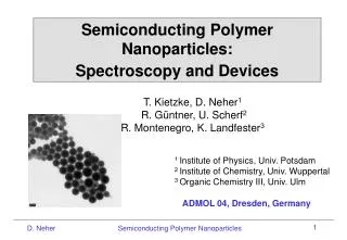
Semiconducting Polymer Nanoparticles: Spectroscopy and Devices. T. Kietzke, D. Neher 1 R. Güntner, U. Scherf 2 R. Montenegro, K. Landfester 3. 1 Institute of Physics, Univ. Potsdam 2 Institute of Chemistry, Univ. Wuppertal 3 Organic Chemistry III, Univ. Ulm. ADMOL 04, Dresden, Germany.

Semiconducting Polymer Nanoparticles: Spectroscopy and Devices
E N D
Presentation Transcript
Semiconducting Polymer Nanoparticles: Spectroscopy and Devices T. Kietzke, D. Neher1 R. Güntner, U. Scherf2 R. Montenegro, K. Landfester3 1 Institute of Physics, Univ. Potsdam 2 Institute of Chemistry, Univ. Wuppertal 3 Organic Chemistry III, Univ. Ulm ADMOL 04,Dresden, Germany
Nanoparticles and nanoparticle polymer layers Blends of nanoparticles – nanostructured layers Blend nanoparticles – phase-separation in nanocontainers Some words about photovoltaic devices
Nobelprize for Chemistry 2000 for the discovery and development of conductive polymers
A D E e- h+ Top Electrode (Al) Top Electrode (Al) - = A Acceptor A Donor D = D + Bottom Electrode ( ITO) Bottom Electrode ( ITO) Substrate Substrate Polymer Blend Bilayer Structure Organic Solar Cells Photogeneration of free charge carriers viaphoto-induced electron transfer DA-device structures
Polymer Blend Layers Coated from Organic Solvents F8BT PFB Confocal Raman: PFB-rich PFB:F8BT ca. 50:50 F8BT-rich PFB:F8BT ca. 20:80 PFB:F8BT (1:1) blend spin-cast from xylene R. Stevenson, D. Richards et al.Appl. Phys. Lett. 79 (2001) 2178 J.J.M. Halls, R.H. Friend et al., Adv. Mater. 12 (2000) 498
Spincoated Blend Layers PFB:F8BT layers spincoated from xylene 1:5 1:1 5:1 PFB:F8BT EQE: 4 % 1.8 % 1.4 % length scale of phase separationdepends on composition H.J. Snaith, R.H. Friend et al., Nanoletters 2 (2002) 1353
One Solution! • One Solution: • coat layer from emulsion of semiconducting polymer nanoparticles (SPNs) Dimension of phase separation defined by particle diameter But you need to find a way to make nanospheres from polymers T. Kietzke, D. Neher, K. Landfester, U. Scherf et al., Nature Materials, June 2003
Nanoparticles and nanoparticle polymer layers Blends of nanoparticles – nanostructured layers Blend nanoparticles – phase-separation in nanocontainers Some words about photovoltaic devices
polymer solution evaporation of solvent ultrasound water + surfactant polymer in organic solvent miniemulsion of polymer solution dispersion of solid polymer particles Alternative Way to Polymer Nanoparticles The size of the particles can be controlled in the range of 50-250nm.
ultrasound Phase I Phase II Miniemulsions polymer + solvent water andsurfactant Polymer Solvent molecule Important condition: Polymer is completely insoluble in water – can not be transferred between droplets Consequence: balance between Laplace pressure and osmotic pressure
Semiconducting Polymer Nanoparticles (SPNs) Tg above decomposition (300 oC) Dispersion under white light Dispersion under UV light (lmax = 365 nm) TEM of nanoparticles Ca. 75 nm diameter K. Landfester, U. Scherf, D. Neher et al., Adv. Mater. 14 (2002) 651
3mm ~100 nm 3mm The material was partially removed to show the monolayer AFM of a LPPP Nanoparticle Layer Layer formed by spin coating a dispersion of LPPP nanoparticles onto a glass substrate. • Particles are closely packed, no cracks can be identified
LED from Aqueous Emulsions Preparation of the LED sample structure: Spin casting aqueous PEDOT/PSS solution Drying Spin casting aqueous LPPP nanosphere dispersion Drying Evaporation of cathodes Thickness: Ca:30nm, Al:80nm
Nanoparticles and nanoparticle polymer layers Blends of nanoparticles – nanostructured layers Blend nanoparticles – phase-separation in nanocontainers Some words about photovoltaic devices
Particle Blend Layers Mix dispersion with polymer A and polymer B particles CN-PF:PMMA (1:1) CN-PF:PMMA (1:2) statistical distribution of particles
R R H 2 H 2 R R 1 1 n R R 1 1 H R 2 Low Tg PF + LPPP Layer Formation of Particle Blends PF forms continuous phase homogenous distribution of LPPP spheres T. Kietzke, D. Neher, K. Landfester,U. Scherf et al., Nat. Mater. 2003
Energy Transfer in Particle Blend Layers PF and LPPP can be excited independently spectral overlap between PF emission and LPPP absorption as-prepared annealed at 200 oC complete transfer of energy in annealed layers
Thermal Stability of Blend Structures mix particles of PF11112 (Tg = RT) and PMMA (Tg=110 oC) different softening temperatures different solubility annealed at 150 oC as prepared annealed at 75 oC
AFM Contour Plots (11 nm Increment) annealed at 150 oC as prepared annealed at 75 oC washed in acetone
Nanoparticles and nanoparticle polymer layers Blends of nanoparticles – nanostructured layers Blend nanoparticles – phase-separation in nanocontainers Some words about photovoltaic devices
PFB F8BT Preparation of Solar Cells Start with solution of PFB and F8BT polymer solution electron donor electron acceptor water + surfactant Nanoparticles which contain both polymers
PFB F8BT Multicomponent Particles Morphology excitation at 380 nm: mainly PFB emission excitation at 462 nm: mainly F8BT emission pronounced asymmetry
Exciplex-Spectroscopy on Multicomponent Particles PFB:F8BT 1:1 A D E e- Recent results by R.H. Friend et al. Exciplex emission at ca. 630 nm Sensitive probe for interface formation Larger exciplex contributionfor spin-coated layers • Morteani, C. Silva, N. Greenham,R.H. Friend et al. Adv. Mater. 15 (2003) 1708
Exciplex-Spectroscopy on Multicomponent Particles largest interface for blend with lowest F8BT concentration weaker exciplex contribution with increasing higher F8BT concentration smaller number of excitons reach interface
Multicomponent Particle Morphology F8BT PFB • F8BT easily penetrates PFB phase,but PFB remains outside F8BT phase • Isolated F8BT phase for higher concentrations • small exciton diffusion length on F8BT (ca. 3 nm)* * M. A. Stevens, C. Silva, D. M. Russel, R. H. Friend,Physical Review B2001, 63, 165213.
Nanoparticles and nanoparticle polymer layers Blends of nanoparticles – nanostructured layers Blend nanoparticles – phase-separation in nanocontainers Some words about photovoltaic devices
PFB F8BT Preparation of Solar Cells Preparation of the solar cells: Spin casting aqueous PEDOT/PSS solution Drying Spin casting aqueous nanosphere dispersion Drying Evaporation of cathodes Thickness: Ca:30nm, Al:80nm electron donor electron acceptor
Solar Cells based on Blend Particles Incident-photon-to-converted-electron efficiency (IPCE) Well-resolved contributions from PFB and F8BT
h h Ca e- e- A h+ h+ ITO Substrate IPCE of Blend Particles 380 nm: PFB 445 nm: F8BT • PFB component most active small exciton diffusion length on F8BT • very small IPCE for 5:1 and 1:5 island formation in particle • highest efficiency for 1:2 asymmetry of particle morphology
at 400 nm illumination Spincoated Blend Layers PFB:F8BT layers spincoated from xylene 1:5 1:1 5:1 EQE: 4 % 1.8 % 1.4 % H.J. Snaith, R.H. Friend et al., Nanoletters 2 (2002) 1353 cylinders of PFB-rich phase dispersed in F8BT rich phase
at 400 nm illumination Interfacial Area in Spincoated Layers Estimate for blend SPNs Interfacial area per film area: with SPNs: optimum conditions achieved but statistics of SPN orientation H.J. Snaith, R.H. Friend et al., Nanoletters 2 (2002) 1353
PPV-based Particle Blend Layers M3EH-PPV CN-Ether-PPV Th. Kietzke, H.H. Hörhold, D. Neher et al., Proc. SPIE 2004, accept. Area = 0.2 cm² 100 mW/cm²
polymer solar cell, Univ. Linz Solar Cells EfficienciesEIPCE cryst.-Si typ. 15-28 % (limit 32 %) 50-80 % wet Grätzel cell 10-12 % 70-80 % polymer/CdSe blend < 7 % 30-50 % polymer/fullerene blend 5 % 60-90 % polymer/polymer laminate 1.8 % 20-30 % polymer/polymer blend < 1.5 % 12-25 %
Conclusion and Outlook • Nanoparticles of conjugated polymers: • fabrication of polymer particles via miniemulsion process • formation of dense solid layers from aqueous media nanostructured polymer layers via particle blends • phase-separation in nanocontainers • control of solar cell efficiencies via particle composition • Outlook: • better understanding of particle morphology • alternative deposition methods components with high electron mobilities single particle properties
A. Heilig Phys. Chem., MPI-KG, Golm H. H. Hörhold University of Jena T. Piok, S. Gamerith, Ch. Gadermaier, F. P. Wenzl, E.J.W. List, University of Graz M. Kumke, H.G. Löhmannsröben University of Potsdam Funding: VW-Foundation, MPG, BMBF, Fond der Chemischen Industrie
