Download
1 / 6
70 likes | 100 Vues
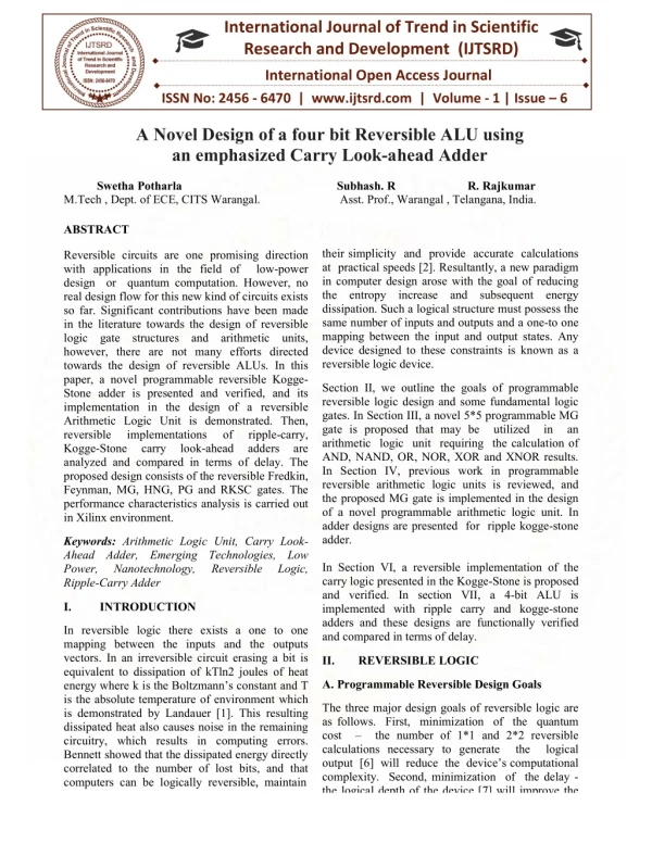
Reversible circuits are one promising direction withapplications in the field of low power design or quantumcomputation. However, no real design flow for this new kind ofcircuits exists so far. Significant contributions have been madein the literature towards the design of reversible logic gatestructures and arithmetic units, however, there are not manyefforts directed towards the design of reversible ALUs. In thispaper, a novel programmable reversible Kogge Stone adder ispresented and verified, and its implementation in the design ofa reversible Arithmetic Logic Unit is demonstrated. Then,reversible implementations of ripple carry, Kogge Stone carrylook ahead adders are analyzed and compared in terms ofdelay. The proposed design consists of the reversible Fredkin,Feynman, MG, HNG, PG and RKSC gates. The performancecharacteristics analysis is carried out in Xilinx environment. Swetha Potharla | Rajkumar R "A Novel Design of a 4 Bit Reversible ALU using Kogge-Stone Adder" Published in International Journal of Trend in Scientific Research and Development (ijtsrd), ISSN: 2456-6470, Volume-1 | Issue-6 , October 2017, URL: https://www.ijtsrd.com/papers/ijtsrd5758.pdf Paper URL: http://www.ijtsrd.com/engineering/electronics-and-communication-engineering/5758/a-novel-design-of-a-4-bit-reversible-alu-using--kogge-stone-adder/swetha-potharla<br>

E N D
International Research Research and Development (IJTSRD) International Journal of Trend in Scientific Scientific (IJTSRD) International Open Access Journal International Open Access Journal ISSN No: 2456 - - 6470 | www.ijtsrd.com | Volume - - 1 | Issue – 6 A Novel Design of a four bit Reversible ALU using A Novel Design of a four bit Reversible ALU using A Novel Design of a four bit Reversible ALU using an emphasized Carry Look an emphasized Carry Look-ahead Adder dder Swetha Potharla M.Tech , Dept. of ECE, CITS Warangal. ABSTRACT Subhash. R R. Rajkumar Asst. Prof., Warangal , Telangana Warangal , Telangana, India. CITS Warangal. R. Rajkumar their simplicity and provide accurate calculations at practical speeds [2]. Resultantly, a new paradigm in computer design arose with the goal of reducing the entropy increase and subsequent energy dissipation. Such a logical structure must possess the same number of inputs and outputs and a one mapping between the input and output states. Any device designed to these constraints is known as a reversible logic device. simplicity and provide accurate calculations at practical speeds [2]. Resultantly, a new paradigm in computer design arose with the goal of reducing the entropy increase and subsequent energy dissipation. Such a logical structure must possess the me number of inputs and outputs and a one-to one mapping between the input and output states. Any device designed to these constraints is known as a Reversible circuits are one promising direction with applications in the field of low design or quantum computation. However, no real design flow for this new kind of circuits exists so far. Significant contributions have been made in the literature towards the design of reversible logic gate structures and arithmetic units, however, there are not many efforts directed towards the design of reversible ALUs. In this paper, a novel programmable reversible Kogge Stone adder is presented and verified, and its implementation in the design of a Arithmetic Logic Unit is demonstrated. Then, reversible implementations Kogge-Stone carry look-ahead analyzed and compared in terms of delay. The proposed design consists of the reversible Fredkin, Feynman, MG, HNG, PG and RKSC gates. The performance characteristics analysis is carried out in Xilinx environment. ing direction of low-power design or quantum computation. However, no real design flow for this new kind of circuits exists so far. Significant contributions have been made in the literature towards the design of reversible logic gate structures and arithmetic units, er, there are not many efforts directed towards the design of reversible ALUs. In this paper, a novel programmable reversible Kogge- Stone adder is presented and verified, and its lementation in the design of a reversible Section II, we outline the goals of programmable reversible logic design and some fundamental logic gates. In Section III, a novel 5*5 programmable MG gate is proposed that may be utilized in an arithmetic logic unit requiring the calculation of AND, NAND, OR, NOR, XOR and XNOR results. In Section IV, previous work in programmable reversible arithmetic logic units is reviewed, and the proposed MG gate is implemented in the design of a novel programmable arithmetic logic unit. In presented for ripple kogge-stone Section II, we outline the goals of programmable reversible logic design and some gates. In Section III, a novel 5*5 programmable MG gate is proposed that may be utilized in an arithmetic logic unit requiring the calculation of AND, NAND, OR, NOR, XOR and XNOR results. In Section IV, previous work in prog reversible arithmetic logic units is reviewed, and the proposed MG gate is implemented in the design of a novel programmable arithmetic logic unit. adder designs are presented for ripple kogge adder. In Section VI, a reversible implementation of the carry logic presented in the Kogge and verified. In section VII, a 4 implemented with ripple carry and kogge adders and these designs are functionally verified and compared in terms of delay. trated. Then, ripple-carry, reversible implementations of of ripple adders adders ahead are are analyzed and compared in terms of delay. The proposed design consists of the reversible Fredkin, Feynman, MG, HNG, PG and RKSC gates. The ristics analysis is carried out Keywords: Arithmetic Logic Unit, Carry Look Ahead Adder, Emerging Technologies, Low Power, Nanotechnology, Ripple-Carry Adder Arithmetic Logic Unit, Carry Look- Ahead Adder, Emerging Technologies, Low Power, Nanotechnology, implementation of the Reversible Reversible Logic, Logic, carry logic presented in the Kogge-Stone is proposed and verified. In section VII, a 4-bit ALU is implemented with ripple carry and kogge-stone adders and these designs are functionally verified I. INTRODUCTION In reversible logic there exists a one to on mapping between the inputs and the outputs vectors. In an irreversible circuit erasing a bit is equivalent to dissipation of kTln2 joules of heat energy where k is the Boltzmann’s constant and T is the absolute temperature of environment which is demonstrated by Landauer [1]. This resulting dissipated heat also causes noise in the remaining circuitry, which results in computing errors. Bennett showed that the dissipated energy directly correlated to the number of lost bits, and that computers can be logically reversible, maintain be logically reversible, maintain one to one mapping between the inputs and the outputs vectors. In an irreversible circuit erasing a bit is equivalent to dissipation of kTln2 joules of heat energy where k is the Boltzmann’s constant and T is the absolute temperature of environment which rated by Landauer [1]. This resulting dissipated heat also causes noise in the remaining circuitry, which results in computing errors. Bennett showed that the dissipated energy directly correlated to the number of lost bits, and that II. REVERSIBLE LOGIC A. Programmable Reversible Design Goals A. Programmable Reversible Design Goals The three major design goals of reversible logic are as follows. First, minimization of the quantum cost – the number of 1*1 and 2*2 reversible calculations necessary to generate the logical output [6] will reduce the device’s computational complexity. Second, minimization of the delay the logical depth of the device [7] will improve the the logical depth of the device [7] will improve the The three major design goals of reversible logic are as follows. First, minimization of the quantum the number of 1*1 and 2*2 reversible calculations necessary to generate the logical output [6] will reduce the device’s computational minimization of the delay -
International Journal of Trend in Scientific Research and Development (IJTSRD) ISSN: 2456-6470 ancillary inputs and garbage outputs - inputs and outputs not implemented in the design of the gate and only serve to maintain reversibility of the device will improve the design space require to implement the logic. The third type of fundamental 2*2 reversible logic gate is the integrated qubit gate. This gate is implemented with a Feynman gate with either a Controlled-V or Controlled V+ gate. The XOR output of the Feynman gate is used as the control signal for the Controlled-V or V+ gate it is coupled with. The quantum cost of the integrated qubit gate is 1 and its worst-case delay is 1. The quantum configurations of these gates are shown below in Fig. 3. A programmable reversible logic gate is defined in [8] as a logic structure which possesses a bijection between input and output states and an equal number of inputs and outputs wherein a subset of the inputs are fixed select lines, and a fixed subset of the outputs produce guaranteed logical calculations. An ideal programmable reversible logic gate with j inputs and outputs has a quantity of fixed select inputs m, fixed select outputs n, data inputs d and propagated outputs p such that |d-p|=|m-n| [8]. In addition, an ideal programmable reversible logic gate with m select inputs may produce at maximum n*2^m logical calculations on the n logical outputs. Fig 2: Quantum Representations of Integrated Qubit Gates The 3*3 Peres gate was proposed by Peres in [12]. The Peres gate has a quantum cost of 4 and a worst- case delay of 3. The quantum representation is shown in Fig. 6. The output states map to the inputs in this manner: P=A, Q=A B and R=AB C. B. Fundamental Logic Gates There are three types of fundamental 2*2 reversible logic gates. First, the square-root-of-not gates utilize the unitary operators to produce reversible logic calculations. The and the Controlled-V+ gates are the two types of square-root-of-not gates. In both of these gates, when the control input is 0, the second input is propagated to the output. The same holds for two Controlled-V+ gates in series. There are three 3*3 fundamental reversible logic gates. The first was proposed in [10] by Fredkin and Toffoli. The Fredkin gate’s outputs states map to the inputs as follows: Controlled-V P=A, Q=A B Therefore, the outputs serve as a multiplexed output of the two data inputs based on the control input. It is realized using 2 Feynman gates, a Controlled-V gate and two integrated qubit gates. AC and R=AB A C. When a Controlled-V and Controlled-V+ gate are activated in series, they act as an identity. Toffoli proposed the second fundamental 3*3 reversible logic gate in [11]. The output states of the Toffoli gate map to the inputs in this manner: P=A, Q=B and R=AB C. The quantum cost is 5 and the worst-case delay is 5. The quantum representation is shown below in Fig. 5. The second type of fundamental 2*2 reversible- logic gate is the Feynman gate, or the Controlled- Not gate. Proposed in [9] by Feynman, it is configured such that its outputs states correlate to the input states in the following manner: P=A and Q=A B. The resulting value of the second output corresponds to the result of a conventional XOR gate. Since fanout is expressively forbidden in reversible logic, since a fanout has one input and two outputs, the Feynman gate may be used to duplicate a signal when B is equal to 0. Its quantum configuration is shown in Fig 2. Fig 3: Quantum Representation of Fredkin gate Fig 1: Quantum Representation of Feynman gate Fig 4: Quantum Representation of Toffoli gate
International Journal of Trend in Scientific Research and Development (IJTSRD) ISSN: 2456-6470 The 3*3 Peres gate was proposed by Peres in [12]. The Peres gate has a quantum cost of 4 and a worst-case delay of 3. The quantum representation is shown in Fig. 6. The output states map to the inputs in this manner: P=A, Q=A C. Fig 5: Quantum Representation of Peres gate The HNG gate, also designed by Hagparast and Navi and proposed in [13], is a full adder with inputs A,B,C,D producing outputs P=A, Q=B, R=(A B) C and S=(A shown in B and R=AB Fig. 8: Quantum Representation of the MRG Gate III. PROPOSED REVERSIBLE MG GATE 5*5 PROGRAMMABLE Next, we propose the design of a 5*5 programmable reversible logic gate structure utilized in the implementation of an ALU. Fig. 9 shows the block diagram of the MG, and the logical calculations based on the programmable inputs are presented in Table 2. The cost of the MG is 7, and the worst-case delay is 7. The design for the programmable MG was verified and simulated using VHDL in Xilinx. B)C (AB Fig. D) and is 6. Fig 9: Quantum Representation of Proposed MG. TABLE II Mg Programmable Inputs And Logical Outputs C D E R 0 0 0 A B 0 0 1 A B 0 1 0 A B 0 1 1 A B 1 0 0 A B 1 0 1 A B 1 1 0 A B (AB)' 1 1 1 A B (AB)' IV. MODIFIED ALU DESIGN WITH MG GATE Fig. 6: Hagparast-Navi (HNG) Gate The Peres And-Or (PAOG) gate, proposed in [8], produces the outputs P = A, Q =A C and S=(AB C) ((A shows the quantum representation of the PAOG gate. This gate is an extension of the Peres gate for ALU realization. When the PAOG is utilized as a programmable reversible logic gate with two select inputs, it will calculate four logical calculations on those two logical outputs: AND, NAND, NOR and OR. B, R=AB D). Fig. 7 S AB AB (AB)' (AB)' AB AB T B) A+B (A+B)' (A+B)' A+B A+B (A+B)' (A+B)' A+B Two 1-bit ALUs were proposed in [8]. The first utilizes the MRG gate and HNG gate to produce six logical calculations: ADD, SUB, XOR, XNOR, OR and NOR. The ALU has 8 inputs and 8 outputs. The inputs consist of three data inputs (A, B and Cin) and five fixed input select lines. The eight outputs are: A, S0, S3 and S4 propagated to the output, A SUM, Cout, Overflow and Result. The cost of this 1- bit ALU is 24, and the worst-case delay is 16. For n bit ALU devices, an addition cost of 2 is incurred per bit in order to propagate S1 and S2 to other bits. The proposed in [8], has a quantum cost of 6, since it consists of three XOR gates, 2 Controller-V and one Controller-V+ gate. The worst-case delay of the MRG gate is 6. The quantum representation of the MRG gate is shown in Fig. 8 below. When the MRG is utilized as a programmable reversible logic gate with two select inputs, it will calculate four logical calculations on those two logical Morrison-Ranganathan (MRG) gate, B,
International Journal of Trend in Scientific Research and Development (IJTSRD) ISSN: 2456-6470 The MG gate is utilized in the implementation of a novel arithmetic logic unit based on those proposed in [8]. The ALU, in addition to producing the same logical calculations as the MG, is able to perform addition and subtraction by utilizing the HNG gate and store less-than operation. The cost an n-bit ALU is 37n-3 and had a worst case delay of 4n+13. The proposed ALU is shown in Fig. 10 V. BASIC ADDER DESIGNS The adders implemented are the ripple carry adder and Kogge-Stone adder. The ripple carry adder is one of the simplest adders. It consists of a cascaded series of full adders. The 4-bit ALU implemented by cascading four 1-bit ALUs. The delay for an N-bit adder is given by tadder = (N-1)tcarry + tsum where, tcarry is the carry propagation delay for one stage and tsum is the time required to compute the sum bit for one stage. The Kogge-Stone adder is classified as a parallel prefix adder since the generate and the propagate signals are pre computed. In a tree-based adder, carries are generated in tree and fast computation is obtained at the expense of increased area and power. The parallel-prefix adder becomes more favorable in terms of speed due to the O(log2n) delay through the carry path compared to O(n) for the RCA. Reversible Kogge-Stone Cumulate Logic A reversible carry look-ahead adder based on the Kogge-Stone adder is presented [9]. First, a RKS Cumulate utilized in the calculation of the carry out signal is designed and verified. The logical structure of the RKSC is shown in Fig. 12. The cost of the RKSC is 14 and it has a worst-case delay of 4. VI. IMPLEMENTATION OF REVERSIBLE KOGGE-STONEADDER A reversible Kogge-Stone adder is implemented by using Peres gate as GP block, Feynman gate as Buffer block and RKSC gate as BC block as shown in Fig.13. The design was verified and simulated using VHDL in Xilinx 9.2i. Fig. 12: Reversible Kogge-Stone Cumulate (RKSC) Logical Layout VII. IMPLEMENTATION OF REVERSIBLE KOGGE-STONE ADDER A reversible Kogge-Stone adder is implemented by using Peres gate as GP block, Feynman gate as Buffer block and RKSC gate as BC block as shown in Fig.13. The design was verified and simulated using VHDL in Xilinx 9.2i. Fig.11. 4-bit Kogge-Stone Adder The 4-bit Kogge-Stone adder is built from generate and propagate (GP) blocks, black cell (BC) blocks, and buffer blocks as shown in the Figure 11. The expressions for the output signals g,p generated by the black cell are given by g = gi+pi gj and p = pi pj. The expressions for the output signals g, p obtained by the buffer block are given as g=giand p=pi. The expressions for the output signals g, p obtained by the GP block are given as g=a.b and p=a xor b. Fig 13: 4-bit Reversible Kogge-Stone adder ALU Design with Reversible Kogge-Stone adder The 4-bit ALU was implemented using reversible Kogge-Stone adder as shown in Fig.14. This design was verified and simulated using VHDL in Xilinx9.2i.
International Journal of Trend in Scientific Research and Development (IJTSRD) ISSN: 2456-6470 VIII.COMPARISION AND RESULTS The comparison is carried out in between the reversible Ripple Carry and Kogge-Stone adders with respect to 4-bit ALU design and for those the code was written in VHDL and that was verified and simulated using Xilinx 9.2i. TABLE IV Comparison of ALUs of ripple carry and kogge-stone adders Parameter 4-bit ALU with ripple carry adder Delay(ns) 16.856 LUT’s 37 Fig.14. 4-bit reversible ALU with kogge-stone adder 4-bit ALU with kogge-stone adder 15.536 31 CONCLUSION IX. A novel 5*5 programmable MG gate was proposed and verified that may calculate of AND, NAND, OR, NOR, XOR and XNOR depending on the inputs from the programmer. The proposed MG gate was implemented in the design of a novel programmable arithmetic logic unit. The novel 1-bit ALU required only minimal increase in quantum cost and delay due to the MG design, which also allowed for increased functionality for the programmer. Next, we presented reversible implementations of ripple carry adder (RCA) and kogge-stone adder. A eversible implementation of the carry logic presented in the Kogge tone was presented and verified. The proposed design of 4-bit ALU with RCA and Kogge- Stone adder were compared in terms of delay. REFERENCES 1)R. Landauer, "Irreversibility Generation in the Computational Process," IBM Journal of Research and Development, vol. 5, 1961, pp. 183-91. Fig.15. 1-bit reversible ALU and Heat Fig.16. 4-bit reversible kogge-stone adder 2)C. Bennett, "Logical Reversibility of Computation," IBM Journal of Research and Development, vol. 17, 1973, pp. 525-532. 3)R. Feynman, "Simulating Physics with Computers," International Journal of Theoretical Physics, 1982. Fig.17. 4-bit reversible ALU with ripple carry adder 4)R. Feynman, "Quantum Mechanical Computers," Foundations of Physics, vol. 16, iss. 6, 1986, 5)E. Fredkin and T. Toffoli, "Conservative Logic," International Journal of Theoretical Physics, vol. 21, 1980, pp. 219-53. [6] T. Toffoli, "Reversible Computing," Technical Report MIT/LCS/TM-151, 1980. Fig.18. 4-bit reversible ALU with kogge-stone adder 6)A. Peres, “Reversible Logic and Quantum
International Journal of Trend in Scientific Research and Development (IJTSRD) ISSN: 2456-6470 9)E. Fredkin and T. Toffoli, "Conservative Logic," International Journal of Theoretical Physics, vol. 21, 1980, pp 219-53 1985, pp. 3266-3267. 7)M. Morrison and N. Ranganathan, "Design of a Reversible ALU Programmable Reversible Structures," To Appear International Symposium on VLSI, 2011. Based on Novel Gate IEEE 10)T. Toffoli, "Reversible Computing," Technical Report MIT/LCS/TM- 151 , 1980. Logic in the 11)A. Peres, “Reversible Logic and Quantum Computers,” Physical Review, vol. 32, iss. 6, 1985, pp 326 . 8)R. Feynman, "Quantum Mechanical Computers," Foundations of Physics, vol. 16, iss. 6, 1986, @ IJTSRD | Available Online @ www.ijtsrd.com | Volume – 1 | Issue – 6 | Sep - Oct 2017 Page: 1301